Intro
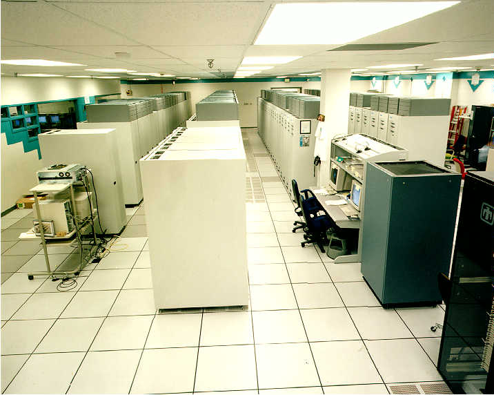
Modern GPUs are ferociously powerful compute engines. The RTX 4090 (NVIDIA’s latest consumer GPU) can perform a theoretical 1.3 teraflop/s of FP64 compute, which is about the same as ASCI Red, a $70M, 1600 sq ft, 104 cabinet supercomputer that was active until 2006 [1][2]. This comparison is actually heavily biased towards ASCI Red (below) because the 4090 is optimized for lower precision arithmetic. It blows my mind that this supercomputer from just ~20 yrs ago is FLOP for FLOP, about as performant as a box that fits in one hand!
The performance characteristics of GPUs are a bit misunderstood, as they are fundamentally throughput machines, and not latency optimized. One common statement I have read online surrounds how much ~faster~ GPUs are than CPUs. A table comparing memory and arithmetic latency for a modern CPU and GPU are below.
By most metrics, CPUs are significantly lower latency (faster) than GPUs. Another metric we could compare with is thread to thread communication latency. Just to make a point, lets compare communication overhead between threads on separate CPU cores/separate GPU streaming multiprocessor.
A CPU can accomplish this in just 59ns [7], while this parameter is undefined for the other camp because there is no mechanism for direct communication between SMs in GPUs! What good are GPUs for then? While GPUs may have high latency and lack robust inter-block communication, they have vastly greater chip die-area dedicated to arithmetic as compared to scheduling/caching on CPUs. This allows GPUs to excel in workloads that involve little serial communication but lots of arithmetic. A great analogy is that of GPUs being a school bus, and CPUs being a sports car. When a school bus is full and moves from point A to point B, it achieves great person-miles/hour metrics. A sports car on the other hand, can move from point A to point B much faster than the school bus but cannot compete in person-miles/hour. While we don’t traditionally think of school busses as particularly ‘fast’, if utilized correctly, they can certainly provide person-miles/hour metrics that not even the fastest race cars can come close to.
GPUs and Deep Learning
In 2012, a team from the University of Toronto smashed records in a global academic computer vision challenge known as ImageNet [8]. Prior to this result, most of the CV community had tackled this challenge using hand-engineered feature detectors and traditional machine learning algorithms. Alex K, Ilya S. and Geoff H. showed however, that an artificial neural network fed with sufficient data and compute could learn features that performed far better than hand-engineered approaches could achieve. One could argue, that the breakthrough in the AlexNet paper was not algorithmic or terribly novel in its nature (Yann LeCun had shown conv nets programmed with back-prop worked in 1989 [9]) but was largely enabled by Alex K’s expertise in GPU programming*. This breakthrough is what lit the explosion of recent DL progress and while the ingredients for the AlexNet breakthrough had been around for a while, what had been missing was the computational power to train a large enough neural net to digest the entire ImageNet dataset, coupled with GPGPU (general purpose GPU) code to make the neural net go brrr.
Deep Learning has characteristics that are very ideal for filling up our big GPU school bus with lots of data and learned parameters! Specifically, the conv net that the UofT team trained involved large amounts of highly parallel arithmetic (matrix multiplies). In the decade since then, artificial nets have digested ever larger datasets on even larger GPU clusters and smashed records in practically every problem with an input-output relationship not easily defined deterministically. While there have been waves of various neural net architectures since 2012 (CNNs, RNNs, Transformers, SSMs, etc) the core DL ingredient of lots of matrix multiplies has not changed much. Over the next many posts on this website I’ll be sharing my learnings on deep learning inference optimization enabled by an understanding of GPU architecture. While these posts focus on NVIDIA GPUs and use CUDA, the general concepts of parallel-programming apply to any GPU based architecture.
Its worth noting that GPUs are certainly not the only way to accelerate deep learning workloads, and will be competing against other approaches over the next several years. Notable contenders include TPUs (Google), Dojo/AP car computer (Tesla), WSE (Cerebras), Grayskull (Tenstorrent), IPUs (Graphcore), and something with analog memresistors (Rain). While I have thoroughly enjoyed learning about GPUs over the past month, I am actually quite bearish on GPUs (and really anything based on the Von Neumann architecture) for DL inference projecting into the far future. I am in the camp that believes biological neural nets, at a high level of abstraction, aren’t all that different from artificial nets. Lets run with this thinking: imagine if every time a biological neuron fired and the action potential reached the synpase, our brains had to go run somewhere (thousands of neurons away) to figure out what ‘weight’ is associated with this connection. Our brains would be horribly inefficient! But this is basically what modern GPUs are doing, utilizing lots of energy on this memory movement, and spending relatively little on the compute itself. Analog approaches with weights implemented in hardware will take time to figure out and scale but will better suit the task of doing lots of dot-products when compared to their digital equivalents. A fun thought experiment is that of a DL accelerator built from very tiny mechanical springs. The law which governs spring behavior (Hooke’s Law, \( F = kx \)) has the same form as the input to an artificial neuron (\( y = wx \)). One could imagine hooking up compressive/tensile springs with different stiffnesses (weights) to plates (neurons) and implementing a ReLU non-linearity by preventing these plates from displacing in the negative direction. If you scaled this out you’d have an incredibly energy efficient mechanism for neural net inference! All you’d have to do is modulate the input plates and measure the position of the output plates, with the only energy losses being minimal heat generation from internal spring stresses. I am not saying this is practical, but it goes to show how elegant and universal the idea of the neuron is. It’s quite unlikely that GPUs are the final stop in the quest for a computational substrate capable of artificial general intelligence.
Memory
Global memory, the largest of all memory types on GPUs, is implemented with Dynamic Random Access Memory (DRAM). These DRAM banks are stored off-chip.
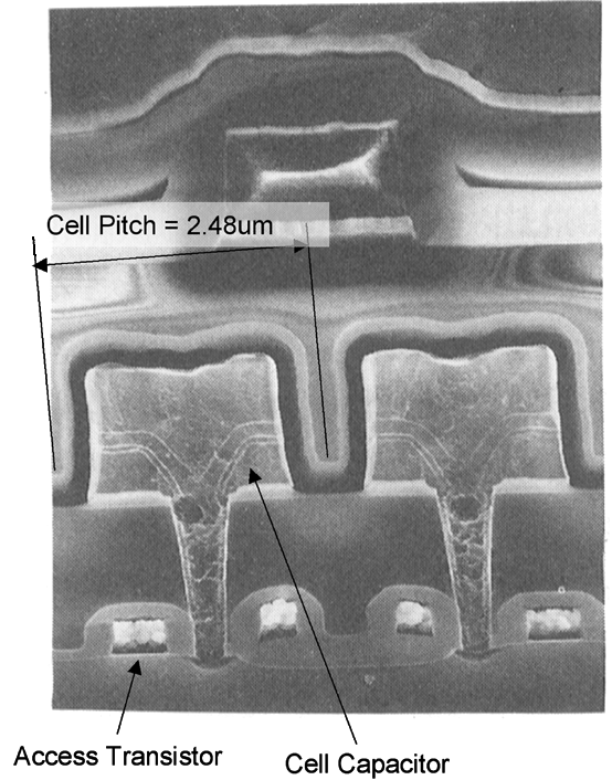
Each bit in DRAM is stored with a capacitor, which stores charge to represent a 1 or 0, and a transistor, which controls read/write access to the capacitor. The transistors for each of these cells are then connected to a bit-line and a word-line. Since capacitors leak charge over time, DRAM cells require constant refreshing, typically at a frequency of ~20Hz for each row.
The word-line is responsible for selecting which row of a DRAM grid to index, while the bit-line allows for column selection and carries the actual 1 or 0 to the row-buffer for the read operation to complete. When a read is performed, the row-buffer is initially precharged to a known neutral value (~0.5V) so as not to corrupt the resulting charge post word-line activation. Next, the word-line is activated, pulling all the bits from its row into the row-buffer. Each bit-line is linked to a sense-amplifier in the row-buffer which converts the small potential difference resulting from being connected to the bit-capacitor into a full digital 1 or 0. This amplified value is used to both rewrite the bit back into the capacitor (since it was just drained) and pass on this value to the memory controller. Its important to note that since activating a word-line pulls all the bits from that row into sense amplifiers, sequential reading of bits is much more efficient than reading bits across separate rows. When a different row has to be accessed, the memory controller has to perform the time consuming steps of pre-charging the row buffer to a neutral potential and activating a new word-line. For this reason, truly ‘random-access’ of DRAM can significantly bottleneck memory throughput.
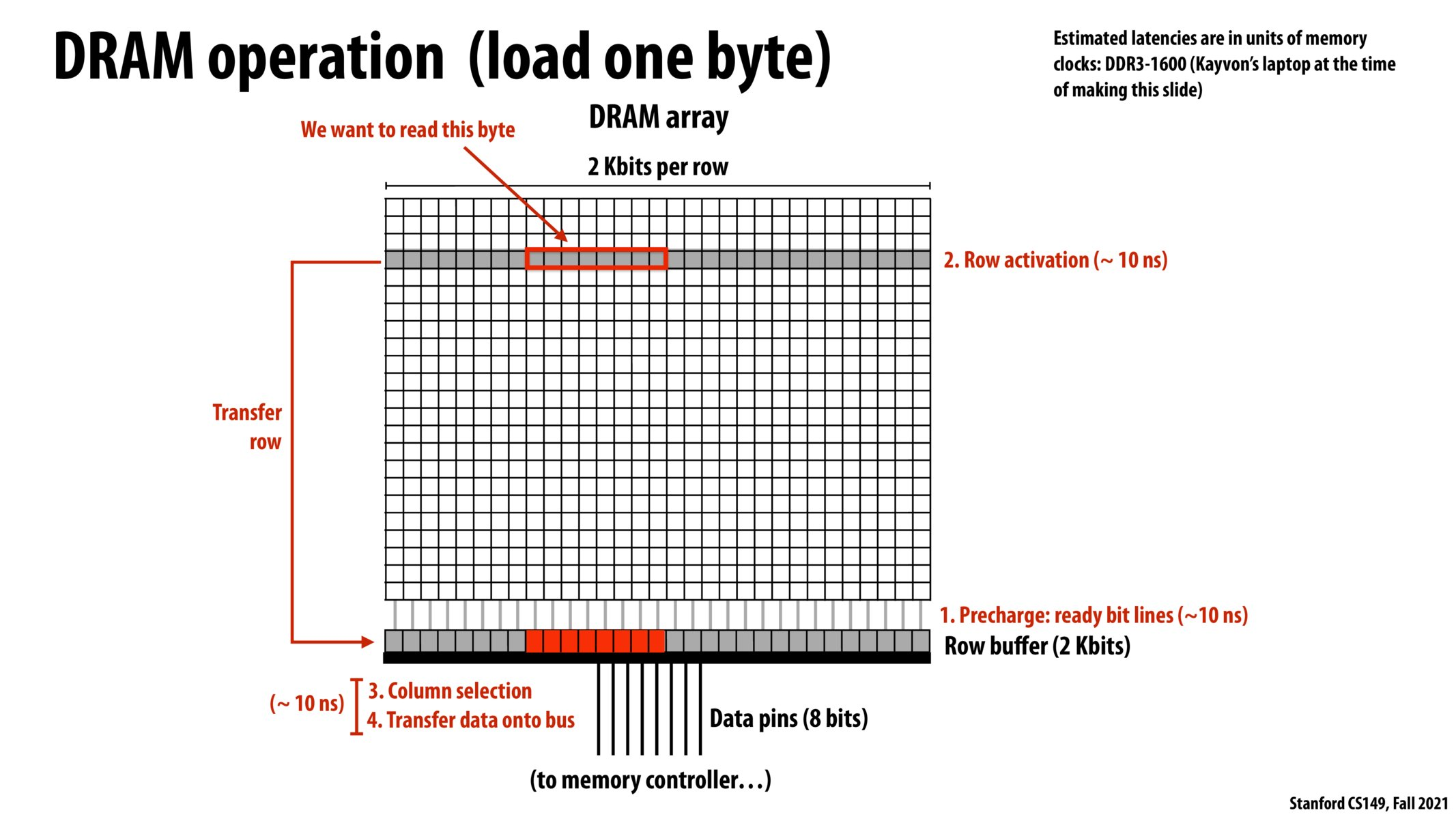
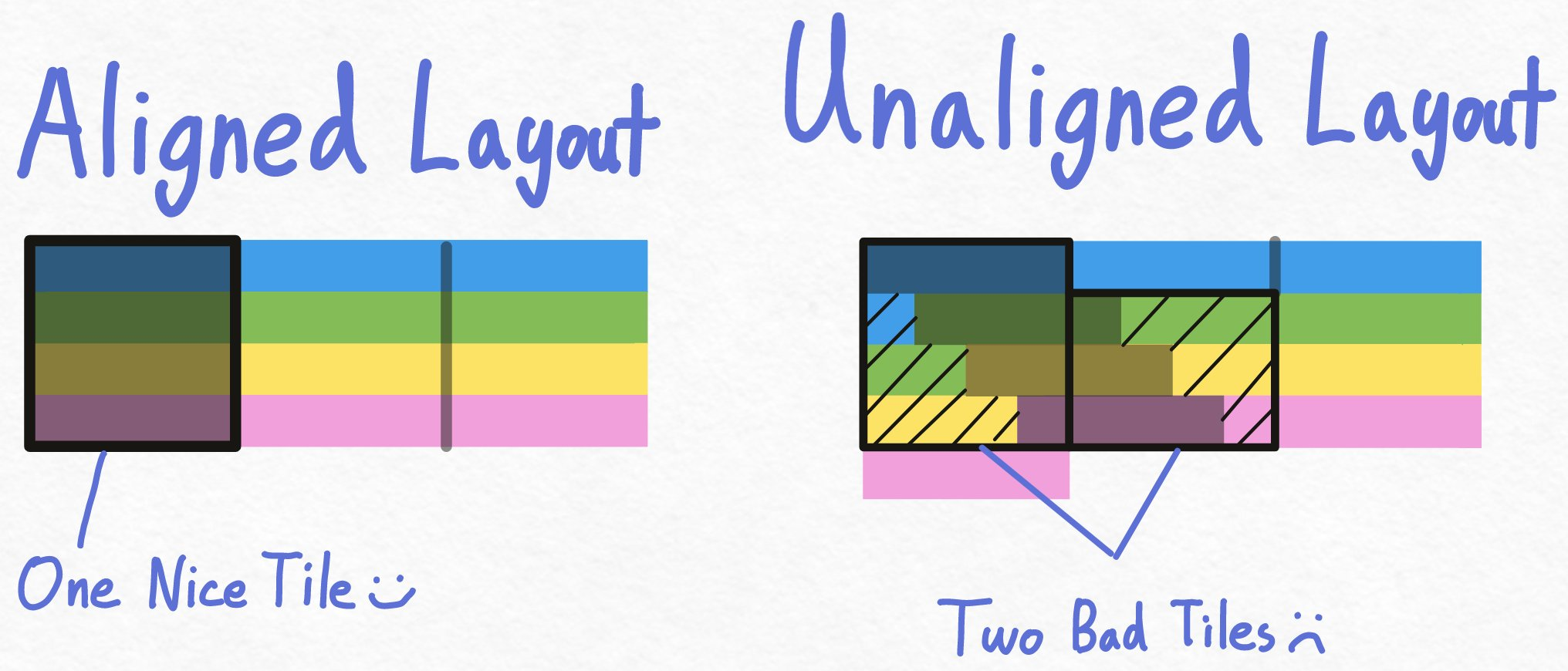
Once a row has been loaded into a buffer, the memory controller processes memory transactions into L2 cache according to transaction sizes known as ‘cache lines’. Another important global memory concept to keep in mind is that of memory alignment. As we discussed, having to read multiple rows in DRAM to access data is pretty undesirable. Depending on how the logical memory placement aligns with the physical memory banks, unaligned layouts may result in excess cache-line transactions/row-buffer loads or possibly both. In practice, you never really have to think about row-buffers when trying to optimize global memory access in CUDA kernels, you just try to touch as few cache-lines as possible with each load. In the case of my RTX 3090, this comes out to making as few 128byte aligned loads from global memory as possible.
SRAM on the other hand is the type of memory that all other memory stores on a GPU are made of. It typically consists of four transistors in a cross-coupled inverter circuit, along with two transistors to serve as read/write gates, totalling six transistors total. The inverter circuit is designed to be a stable bistable circuit and can take on a value of 1 or 0, which it will store perpetually as long as the transistors are still powered. As a result, SRAM does not need constant refreshing like DRAM, however the storage is still volatile and information is lost when power is cut to the SRAM cell. The advantage of SRAM over DRAM is significantly lower memory access latency. This comes at the cost of having a much larger die-footprint than an equivalent DRAM cell (1 transistor and capacitor vs. 6 transistors) and also having a higher on-state power draw. In theory, SRAM cells should not suffer from the drawbacks of non-sequential access that DRAM suffers from, but in practice this isn’t entirely the case.
The programmer managed SRAM on NVIDIA GPUs, commonly referred to as ‘Shared Memory’, is divided into 32 banks of on-chip SRAM cells. While shared memory access across different banks does not see a drop in throughput when bits are accessed randomly or sequentially, each bank does have a limit of serving 1 byte per clock cycle. As a result, it is most efficient to have each thread access sequential shared memory addresses to prevent accesses from becoming serialized. It should be noted that this latency penalty arises due to resource contention between threads trying to access the same memory pool and not due to the ordering of memory addresses within the same pool.
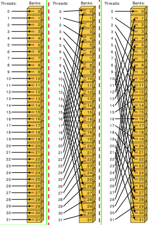
In the example above, the access pattern on the left and right are bank-conflict free. Notice on the right that despite each thread accessing banks haphazardly, they incur no performance penalty. The pattern in the middle however, involves multiple threads simultaneously accessing the same SRAM bank. The SRAM memory controller in this case would have to serialize these accesses and the net result would be the access being twice as slow.
Memory Hierachy
Memory on a GPU is fragmented in a hierarchy where each level trades off latency and throughput for capacity. This trend of trading off latency for memory size is common in processors and due to larger memory banks necessitating more complex indexing circuitry as well as longer signal path lengths .
The largest/slowest memory on a GPU is global memory, which, like mentioned earlier resides off chip. These DRAM banks are meant to be accessible by any thread on any streaming multiprocessor.
One step down from GMEM is the L2 cache. The L2 cache is managed by the GPU and serves as an intermediary between streaming multi-processors and GMEM access. In Ampere GPUs the L2 is actually formed by two separate physical memory stores and latency for half of the SMs to the farther L2 partition isn’t that much better than accessing global memory. The L2 allows frequently accessed GMEM cache-lines to be closer to the SMs and also intercepts data spilling out of thread registers.
Also on the SM lies the L1 Cache/Shared Memory. The L1 and SMEM are actually the same physical memory and the programmer can trade off more SMEM for less L1 and vice-versa. Shared memory is entirely programmer managed, while L1 operates similarly to the L2 and stores data based on what the hardware deems is most likely to result in a cache hit. Shared memory use is critical to writing high performance GPU kernels! Since shared memory can be accessed by all threads in a block, it can support relatively complex serial operations, such as a sum-reduction. Shared memory can also be useful for coalescing a strided global memory load, which if performed directly into thread registers may have required very slow un-coalesced access. While shared memory access latency is drastically better than L2 or GMEM access, it is an order-of-magnitude smaller in capacity than L2 and and three OOMs smaller than GMEM. As a result, it can be a bit tricky to manage SMEM allocation while maintaining high occupancy. Overusing SMEM will prevent the warp scheduler from making the SM fully occupied and hurt overall kernel performance.
Finally, we had thread registers. These are programmer managed and allocated for each thread. They are much faster than shared memory and are typically the memory cells that are loaded from when executing arithmetic instructions. On an RTX 3090, threads cannot use more than 255 registers without spilling to ‘local memory’ which is somewhat deceptively named as it refers to an address space that threads can utilize in global memory. Obviously this can have negative performance consequences and should be avoided.
Below is a brief description of the various GPU memory stores and their characteristics on an RTX 3090 (Ampere based GPU).
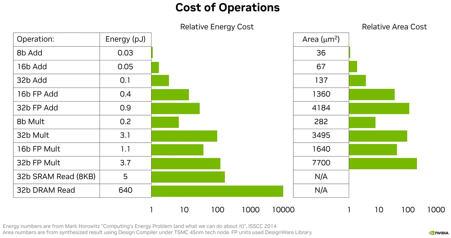
I was curious as to how much of global memory latency can be accounted for by the time it takes for electrons to travel from on-chip to DRAM modules off-chip. Even assuming very liberal estimates for signal path length, physical travel time (I don’t think) is a huge factor in memory access latency. I imagine the bigger inputs are things like transistor gate capacitance, finite memory bus width, clock speed, and number of nodes between each endpoint.
Speed of Electrons in Copper - ~16cm/ns
Path Length - 25cm
Signal Propagation Delay - ~1.6ns
Compute
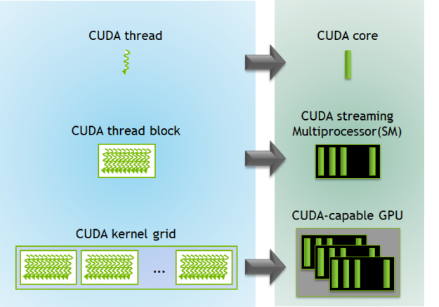
Before going into details about hardware, it’s useful to understand the primary programming abstractions in CUDA. All compute with the same global memory space is encapsulated in a kernel (not strictly true but lets run with this). Within a kernel, there exist ‘grids’ of ‘blocks’, which in turn consist of up to 1024 threads. Each block runs on the same streaming multiprocessor (define this) and all threads within the same block have access to the same shared memory. Blocks run entirely independent of other blocks (not really, clusters are a thing and so are atomics) so any computation that involves serial dependencies needs to be completed within the same block. When the hardware actually executes threads in the block, they are ran 32 at a time in a ‘warp’. Warp execution follows the single-instance multiple-data (SIMD) model, meaning the every thread in the warp gets the same instruction at the same time but each thread acts on different data. (not entirely true because of warp divergence).
The SM persists all relevant thread memory during the course of its execution, which enables zero-cost task switching. In contrast when CPUs switch threads or processes, there is overhead associated because CPUs save thread state in slower memory caches to enable the task to be resumed later on. During task resumption, these state variables have to be brought back from the slower memory caches into faster register files (need to define this). On GPUs, however, warp variables are all kept in the register file when execution switches to a different warp. This makes it so any warp can swap back in and pick right back up where it left off. Often times warps will utilize a large number of registers and then ‘stall’ due to memory dependencies. When the cumulative size of all register files for issued warps exceeds the physical register space on the SM, this can lead to ‘register spilling’. In these cases the GPU will fall back to storing local variables in L2 cache or global memory. The key takeaway here is that the GPU is designed to very quickly swap in different workloads to hide memory latency (define this on the side). So long as there are enough warps to throw into the fray, memory loading and compute can overlap. It’s the programmers job to understand this concept (occupancy) and make sure the GPUs compute execution units can keep the hungry compute units fed.
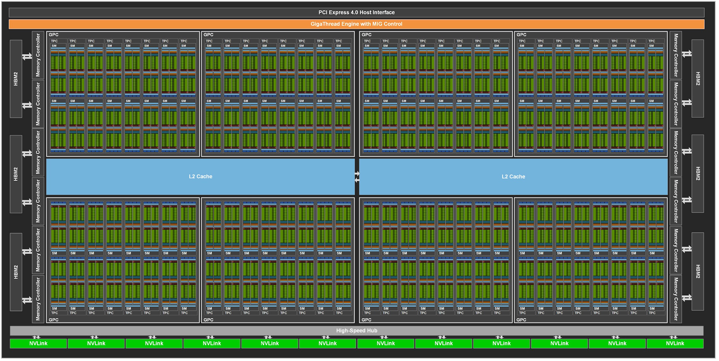
NVIDIA’s hardware architecture has evolved quite drastically over the past decade, and continues to do so with many new features in the most recent Hopper architecture. I personally use an RTX 3090 which is part of the ‘Ampere’ family. The Ampere architecture based GA102 chip includes a whopping 28.3 billion transistors on a die-area of 628 mm^2. This is more transistors than on every single MOS 6502 inside every Apple II put together… The three main compute resources include
10,752 CUDA Cores
Ray Tracing Cores (these are actually primarily for real-time graphics ray tracing so we don’t care too much about them 😛)
336 Tensor Cores
The actual execution of GPU kernels happens on 84 separate ‘streaming multi-processors’. Each SM has 128 CUDA cores and 4 tensor cores. Since 32 threads consist of a warp and there are 128 CUDA cores, each SM can execute 128 threads worth of instructions concurrently. Diving into SM architecture, we find each SM consists of four segments, each of which has:
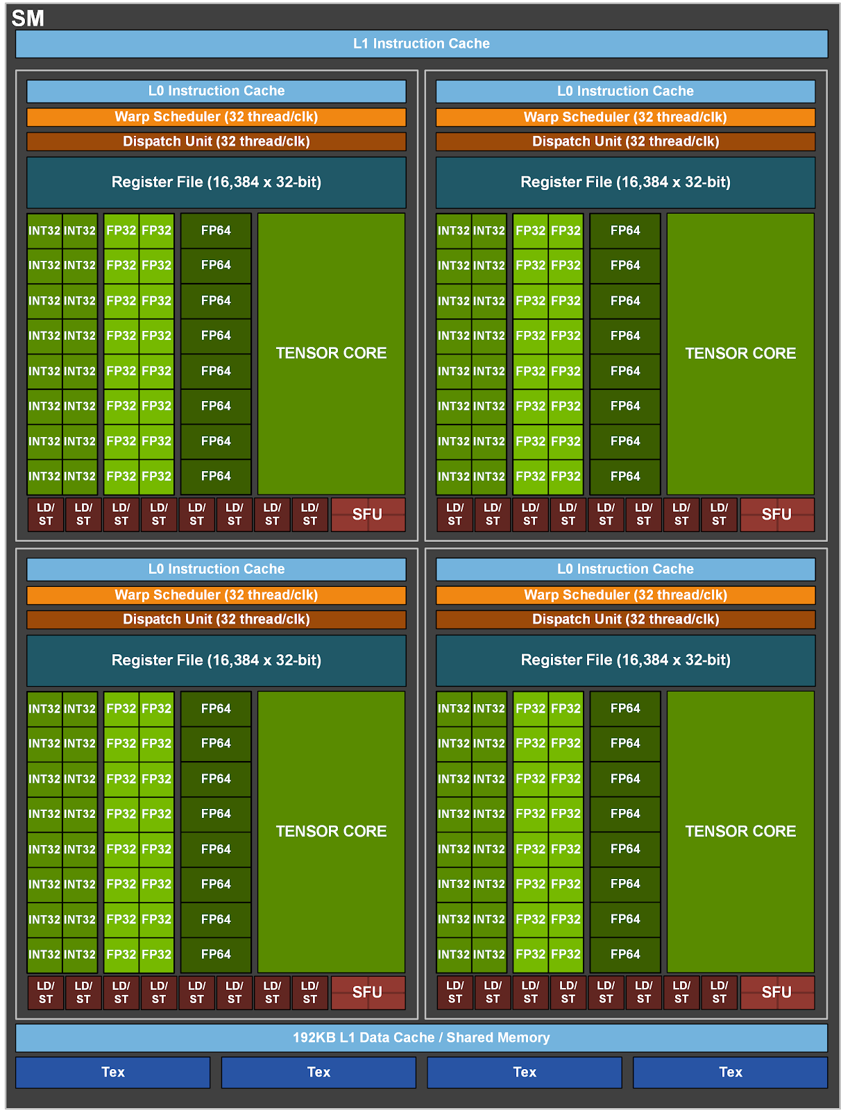
L0 Instruction Cache - Holds local copies of instructions that the processor is likely to excute.
Warp Scheduler - Manages execution of warps in SIMT (single instance multi thread) fashion.
Dispatch Unit - Sends actual instructions to execution units (FP32/tensor-core/etc).
65.536 KB Register File - Stores per-thread variables and program state.
32 FP32 ALUs - Performs FP32 operations (add/multiply/fused multiply accumulate)
32 INT32 ALUs - Performs INT32 operations
8 FP64 ALUs = Performs double percision operations
8 Load/Store Units - Handles memory accesses to shared, global, constant, and local address spaces.
The instruction execution model that NVIDIA GPUs follows is something NVIDIA calls SIMT (single instance multi-thread). In this model, at every clock cycle -
- the warp scheduler selects a warp that is not stalled, and sends one or two instructions for that warp to the dispatch unit
- the dispatch unit in turn sends instructions to the relevant execution units. assuming there is no warp divergence (instances where threads in a warp follow different code execution paths), the unit will send 32 instructions/clk cycle, each mapping to a different thread/data-point.
The ability to send multiple instructions per clock cycle can only happen when there are independent instructions for the same warp which map to different execution units. This could happen, for example, when one part of a thread’s program requires FP32 instructions while another, data-independent part requires using tensor cores. Pre-Volta, each warp on an SM had only one program counter and stack assigned to it. When warp divergence occured, each diverged path had to be executed serially in their entirety. An active mask (bitmask of threads active for that path) would control whether a thread executed instructions or not.
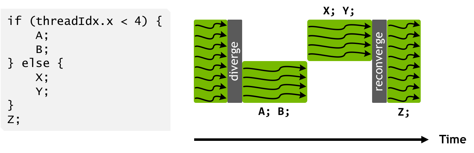
With the introduction of Volta, each thread kept track of its own program counter and call stack, which meant execution of different diverged branches could be interleaved.
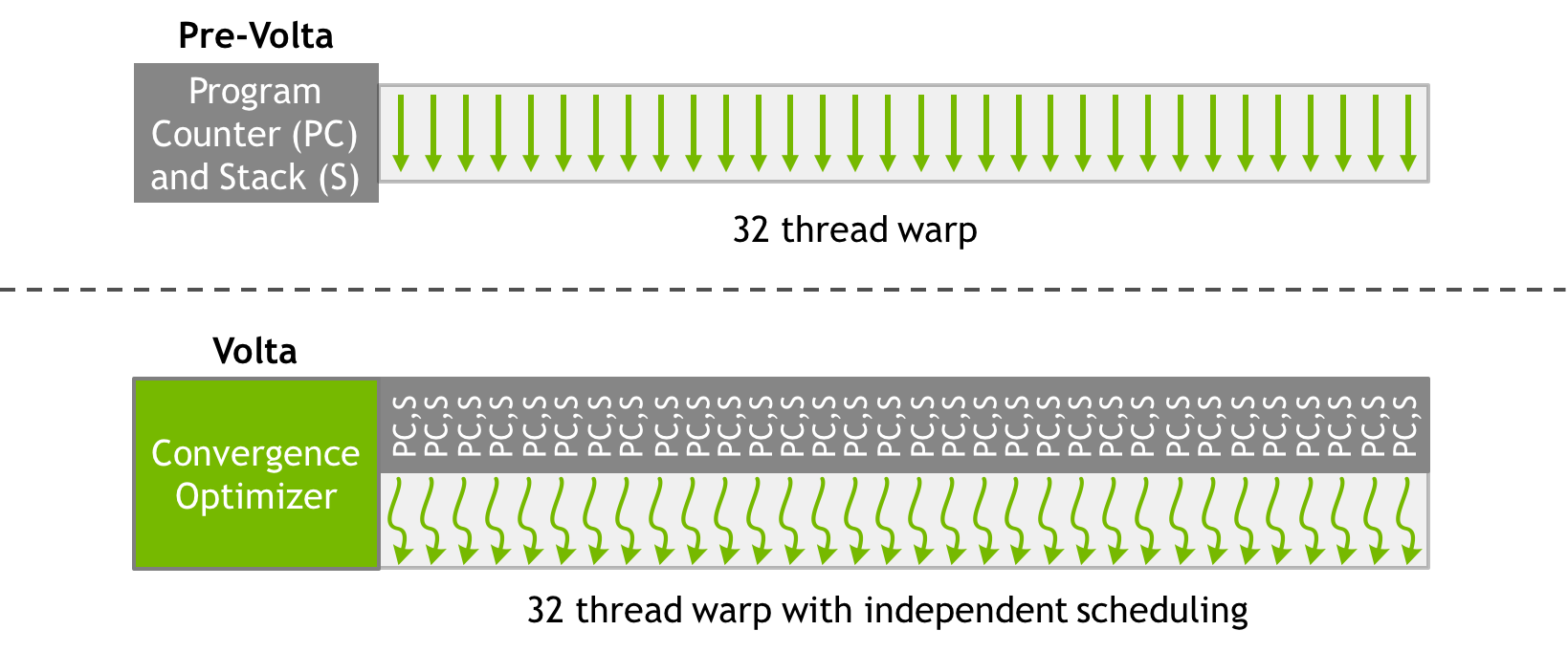
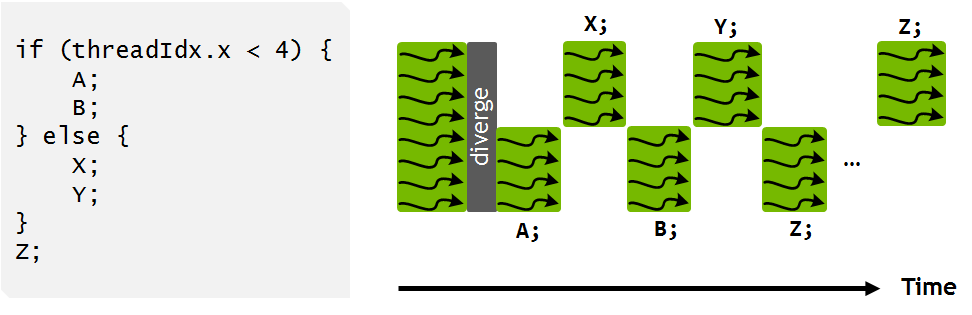
This approach allows for greater instruction-level parallelism and reduces (to some extent) the performance hit of warp divergence. Its important to note that the warp scheduler still follows the SIMT model and can only issue one instruction per clock cycle. Threads in two different branches cannot receive instructions in the same clock cycle, but the warp scheduler and switch back and forth between diverged paths more dynamically.
Tensor Cores
Volta was also the first architecture to introduce a brand new category of execution unit, the tensor core. This hardware is meant to accelerate matrix multiplication for deep learning workloads and is *incredibly * fast. Each tensor core can execute an entire 16x16 mma (matrix multiply and accumulate) in a single clock cycle (~0.75ns for RTX 3090).
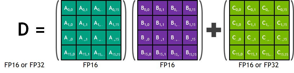
The operation is performed as a warp-wide operation as all 32 threads have to participate in loading the input matrices into the tensor cores, which breaks the thread/warp abstraction to some extent in CUDA. I plan on doing a whole post on these later, so I am not going to include too much detail on the API and hardware implementation for now.
Key Takeaways
Most of what you need to know to optimize GPU inference performance is summed up in the gif below. I should note the gif compares latency, while what we care about is throughput, but it turns out throughput numbers pretty closely match latency numbers so it all works out!
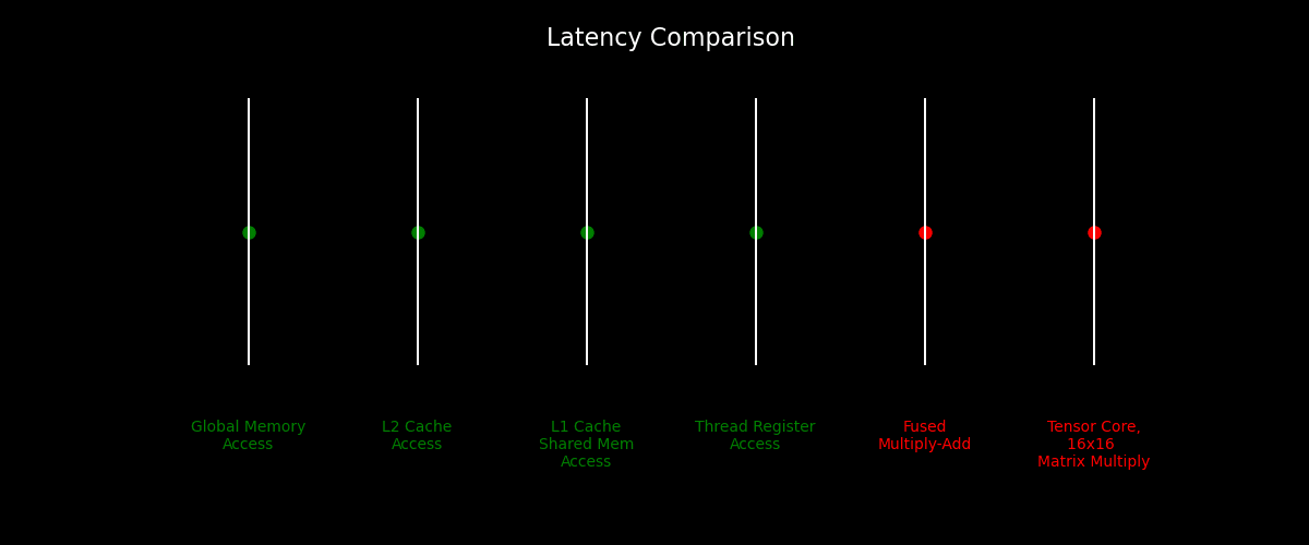
Memory latency in modern GPUs is a killer! Its pretty wild visualizing how slow global memory access is. Minimize GMEM access as much as you can. This next picture shows another ~40% of the picture.
While memory latency is long, efficient use of shared memory/registers and coalesced global memory access can unlock high memory throughput. This in turns allows you to keep the thousands of cores on-chip fed. A kernel with healthy memory usage practices and effective overlapping of memory access with compute will go very far in achieving high overall hardware utilization.
References
[1] https://en.wikipedia.org/wiki/ASCI_Red
[2] https://www.techpowerup.com/gpu-specs/geforce-rtx-4090.c3889
[3] https://www.alibabacloud.com/blog/the-mechanism-behind-measuring-cache-access-latency_599384
[5] https://arxiv.org/pdf/1804.06826.pdf
[6] http://courses.cms.caltech.edu/cs179/Old/2019_lectures/cs179_2019_lec04.pdf
[7] https://chipsandcheese.com/2023/11/07/core-to-core-latency-data-on-large-systems/
[9] https://proceedings.neurips.cc/paper/1989/file/53c3bce66e43be4f209556518c2fcb54-Paper.pdf
[10] https://www.semianalysis.com/p/neural-network-quantization-and-number
[11] https://medium.com/@smallfishbigsea/basic-concepts-in-gpu-computing-3388710e9239
[13] https://gfxcourses.stanford.edu/cs149/fall21/lecture/graphdram/slide_61
[14] https://twitter.com/cHHillee
[16] http://homepages.math.uic.edu/~jan/mcs572f16/mcs572notes/lec35.html
[17] https://developer.nvidia.com/blog/cuda-refresher-cuda-programming-model/
[18] https://www.researchgate.net/figure/NVIDIA-Volta-GV100-SM-16_fig1_353446204
[19] https://developer.nvidia.com/blog/inside-volta/
[20] https://developer.nvidia.com/blog/programming-tensor-cores-cuda-9/
[21] https://www.nextplatform.com/2020/05/28/diving-deep-into-the-nvidia-ampere-gpu-architecture/